To make predictions, artificial intelligence (AI) relies on the processing of large amounts of data and that takes a lot of energy. Imec develops solutions to drastically reduce that energy consumption. A new chip, in which these calculations are performed directly in the memory by means of analogue technology, is a major breakthrough in this field.
In short:
- Artificial intelligence goes hand in hand with high energy consumption as more and more calculations are sent to data centers.
- We could save a lot of energy if we could perform pattern recognition calculations where it makes most sense: on a wireless sensor, a mobile device, or in a car.
- Imec develops extremely energy-efficient hardware to enable this paradigm shift
Our planet’s warming up. Addressing that problem requires a climate transition. This transition is the driving force behind the European Commission’s work programme for 2020, entitled ‘Towards a fair, climate-neutral and digital Europe’. In addition to an ecological transition, we are also facing a digital transition. The digital transformation is therefore the second spearhead of the EU programme, with a particular emphasis on artificial intelligence (AI). When the European Commission states that ‘technologies such as AI will be a crucial factor in achieving the objectives of the Green Deal’, it links both spearheads. The idea behind it: using AI as a weapon in the fight against global warming.
The cost of AI to the planet
Artificial intelligence has a lot of potential, for example, to make more accurate climate forecasts, to detect energy loss or to help decarbonize different industries. On the other hand, the technology itself comes at an ecological cost. After all, it relies on processing huge amounts of data. This already accounts for a substantial part of global electricity production. Moreover, the number of calculations is increasing exponentially. Although these calculations are typically carried out in data centers that have already become much more energy efficient in recent years and partly use renewable energy, the impact on our planet is considerable.
For example, last year researchers from the University of Massachusetts calculated the emissions associated with training models in natural language processing (mainly used to improve translation machines). They did this by briefly testing different algorithms on a single GPU, extrapolating the power consumption with the reported training duration and converting that into CO2 emissions based on the average energy mix at different cloud providers. Conclusion: fine-tuning the most energy-consuming algorithm releases up to 284 tonnes of CO2. This is equivalent to the CO2 emissions of five cars during their entire lifespan, including construction.
A growing awareness is therefore emerging among AI researchers to take more account of the ecological cost of the algorithms they are developing. Recently, researchers have been able to enter their total calculation time and the hardware and cloud service used for this into a Machine Learning Emissions Calculator, after which the estimated CO2 emissions are included in their paper.
To green AI hardware
In essence, you can reduce that ecological footprint in two different ways: via the software and via the hardware. You can try to develop more efficient algorithms that minimize the number of calculations. A typical example is the technique of network pruning. In doing so, you ‘prune out’ all the parts that have little importance for the end result. What then remains is a neural network that has the same functionality, but is smaller, faster and more energy efficient.
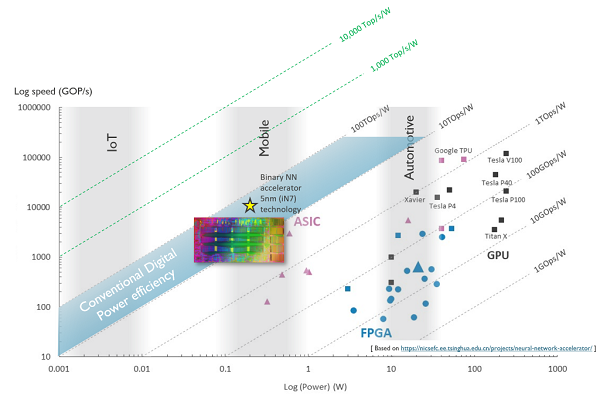
You can also design energy-efficient hardware. Currently, AI calculations are mainly performed on graphical processors (GPUs). These processors are not specially designed for this kind of calculations, but their architecture turned out to be well suited for it. Due to the wide availability of GPUs, neural networks took off. In recent years, processors have also been developed to specifically accelerate AI calculations (such as Google’s Tensor Processing Units – TPUs). These processors can perform more calculations per second than GPUs, while consuming the same amount of energy. Other systems, on the other hand, use FPGAs, which consume less energy but also calculate much less quickly. If you compare the ratio between calculation speed and energy consumption, the ASIC, a competitor of the FPGA, scores best. Figure 1 compares the speed and energy consumption of different components. The ratio between both, the energy performance, is expressed in TOPS/W (tera operations per second per Watt or the number of trillion calculations you can perform per unit of energy). However, in order to drastically increase energy efficiency from 1 TOPS/W to 10 000 TOPS/W, completely new technology is needed.

From cloud to edge
Currently, most of the calculations are sent to the processors of a data center. However, we can also choose to perform (part of) the AI calculations at a different location.
“You can save a lot of energy if you manage to process the data locally,” says Diederik Verkest, program director of machine learning at imec. “The accumulated energy consumption of all data centres in the world is huge, but the amount of energy used to send data from your device to the data centres is about the same. That transmission energy would be avoided if the calculations were performed in the device itself.”
In doing so, we can respond to an evolution that is already in full swing: that of the cloud to the ‘edge’. More and more data is being collected via increasingly smaller devices. If we want to be able to process this data directly on the ‘edge device’, the energy consumption for these calculations must be significantly reduced anyway. How low? “That depends on the size of the device in which they are performed,” explains Verkest. The concept of ‘edge device’ can be filled in in different ways. It can be a small IoT sensor or a mobile phone, but also a self-propelled car. “In a self-propelled car, quick decisions are vital and you don’t have the time to send the calculations back and forth to a data center. So the suitcase is currently packed with GPUs that process the images locally,” says Verkest.
“In the case of image recognition you are talking about twenty trillion operations to classify one object. In a data center you would perform those calculations in a fraction of a second with GPUs that consume around 200 watts. If you are already satisfied with a calculation time of one second to recognise one image, then a GPU of 20 Watts will suffice. This can still be feasible in a car, but for smaller devices this energy consumption is too high. If the battery of your smartphone has a capacity of 4000 mAh, you have 14.8 Wh at your disposal. If we were to run a 20 Watt GPU in there, you would have to recharge your smartphone after less than three quarters of an hour flat. For IoT sensors, where the battery has to last much longer, the use of this kind of processors becomes completely unfeasible. For that segment there are no solutions yet”, says Verkest. “That is why we are now treading completely new paths.
Traditional computer architecture on the shovel
In order for wireless devices to make quick decisions, new computer architectures need to be designed. More specifically, an energy-efficient solution is needed for the forecasting phase. Before an algorithm can make predictions, it must first be ‘trained’. The calculations during this learning phase can just as well be done in advance in the data center. Once the learning phase is over, the smart device must be able to process new data itself in order to make the correct prediction. It is this part of the calculations, the so-called ‘inference’, that will be performed locally.
Suppose, for example, that we have learned an AI system to distinguish a cat from a dog. This means that we have given a neural network a lot of animal pictures and we have given it continuous feedback until it has optimized its parameters in such a way that it can make the right prediction. If we now show a new animal picture, then the algorithm can come to a valuable output on its own (for example ‘this is a cat with a 95 percent probability’). During this infestation phase, the system has to plow through large amounts of data. Not only the new cat picture, but also the previously learned parameters are retrieved from the memory. Moving that data takes a lot of energy.
Since the early days of the digital computer era, the processor has been separated from the memory. In the processor operations are performed on data elements that are retrieved from memory. If these operations are performed on gigantic amounts of data, the retrieval sometimes takes longer than the time needed to perform the operation. This problem is especially evident in AI calculations, because the infertion phase depends on multiplying large vectors and matrices.
Moreover, each operation is performed with the precision of a digital computer, which also requires a lot of energy. In recent years, however, researchers have found that the end result (pattern recognition) is hardly influenced by the calculation precision with which each individual operation is carried out. You could therefore save energy by performing these calculations as close to memory as possible, with lower precision. That is why Verkest’s research group proposed a new approach that completely overhauls traditional computer architecture: the calculations are performed directly in memory, using analogue technology.
The analogue approach
Integrating an analogue system into a digital system? At first sight this seems like a strange move in a world where everything is digitized. Analogue techniques, which use continuous signals instead of zeros and ones, are intrinsically less accurate. But as said before, performing every operation with high precision is not a requirement to achieve an accurate end result. What’s more, with this analog approach, you can achieve the same result faster and with less energy consumption.
How about that? By using the laws of electrical science, the operations of a matrix vector multiplication can be performed in one go, instead of one after the other. If a voltage is assigned to the input values and a conductance to the taught parameters, then each multiplication corresponds to a current (Ohm’s law). You can add it up (Kirchoff’s law of current), so that the value of the current gives you the result of the matrix-vector multiplication. This way you can do the calculation directly without having to retrieve the parameters over and over again.
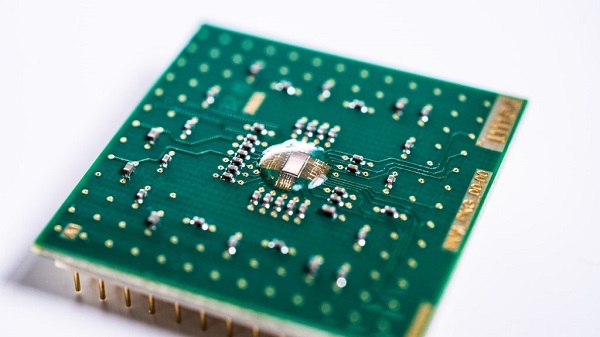
In order to demonstrate that it works effectively in practice, the new architecture has been integrated into a chip. The Analogue Inference Accelerator (AnIA), as the new chip is called, reaches 2,900 TOPS/W, or 2,900 trillion operations per Joule. “This is a reference implementation, with which we want to demonstrate that it is possible to perform analog calculations in memory,” says Verkest. “We can implement this in a compact way and its energy efficiency is already ten to one hundred times better than that of digital chips”.
The ultimate goal is to eventually evolve to 10,000 TOPS/W (10,000 trillion operations per Joule). The concrete path to this goal is described in a recent paper, which proposes a blueprint for the development of such extremely energy-efficient and compact chips. In this way, wireless sensors will be able to autonomously recognize patterns on the data they have collected themselves. It will then no longer be necessary to go back and forth to a data center.

About the Author

Diederik Verkest holds a Ph.D. in Applied Sciences from the KU Leuven (Belgium). After working in the VLSI design methodology group of imec (Leuven, Belgium) in the domain of system-on-chip design, he joined imec’s process technology unit as director of imec’s INSITE program focusing on co-optimization of design and process technology for sub-7nm nodes. Since 2018 he is in charge of imec’s ML program aiming at improving energy efficiency of ML hardware through innovation in circuits and devices.
Sign up for the free insideAI News newsletter.


Speak Your Mind